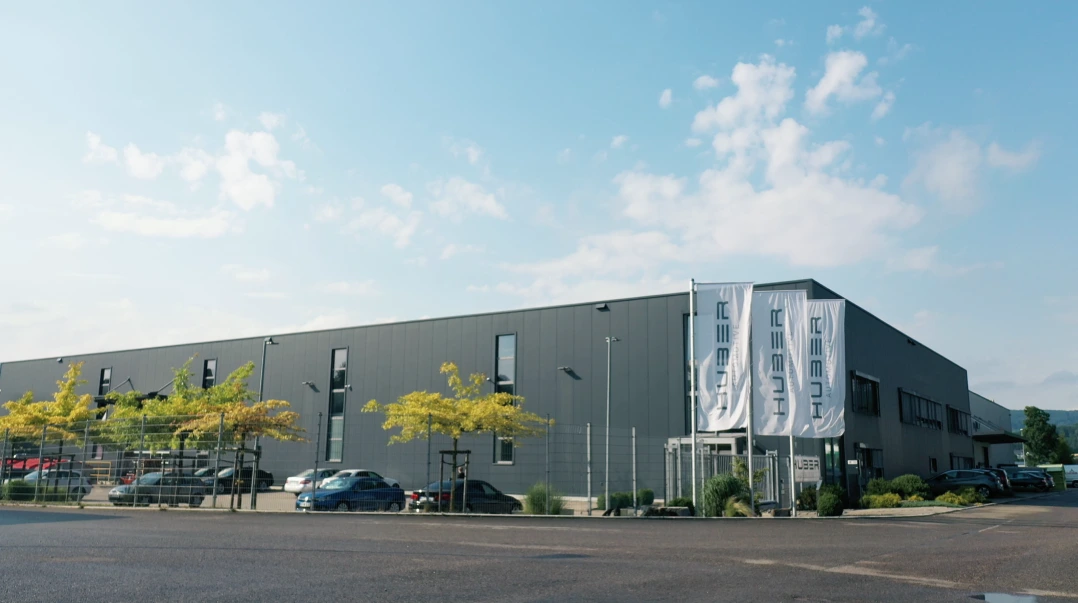
For over 30 years, the Huber Group has been your reliable partner for EMBEDDED ELECTRONICS. From Southern Germany, we serve customers across various industries in Germany and worldwide. At our development center in Mühlhausen, we design and test innovative electronics for both proprietary and customer-specific products. Our two regional production facilities are technologically advanced and equipped to handle modern electronics. This enables us to successfully execute projects ranging from High Mix to High Volume with our EMS services.
Press-Fit Technology
- For connectors
- For plug contacts with force-displacement monitoring
SMT Assembly
- Solder paste printing (including stepped stencils)
- 3D Inline Solder Paste Volume Inspection (SPI)
- Reflow soldering
(Nitrogen atmosphere with or without vacuum) - Automated Optical Inspection (AOI),
before and after reflow process - Through Hole Reflow (THR) technology/Pin in Paste
- Maximum PCB/panel size: L 810 mm x W 490 mm
- Placement precision: 0.025 mm
- Maximum placement capacity: > 1 million CPH (IPC 9850)
- SMD components: up to 0201
THT Assembly
- Machine/manual assembly
- Soldering via selective soldering systems
- Soldering via automated soldering iron systems
- Soldering via mini wave soldering
- Maximum width: 508 mm
- Maximum length: 508 mm
- Max. component height PCB top side: up to 120 mm
- Max. component height PCB bottom side: up to 30 mm
- Max. weight: 8 kg
Highest Precision in Every Production Phase
Let’s bring your electronics projects to success together – with customized EMS manufacturing at the highest level. On request with design review (DFM analysis).
Highest Precision in Every Production Phase – From the initial idea to series production: We bring your electronics projects to life with cutting-edge technology and production expertise. Whether manual THT assembly or highly automated SMT manufacturing for millions of components daily – we deliver customized solutions that combine efficiency and quality. Rely on our expertise for your electronic assembly manufacturing.
Control Unit Manufacturing
Post-Processing and Assembly
Coating (Conformal Coating)
- Underfill (e.g., for BGA)
- Curtain nozzle
- Jet nozzle
- Pasty materials (sealants and adhesives)
- IR drying (inline)
- Hot air drying (batch)
- Optical inspection of coated surfaces (CCI)
- Coating thickness measurement (cross-section measurement)
Final Assembly
- Panel separation (milling)
- Manual to fully automated final assembly
- Application of sealants
- Leakage & functionality testing
PCBA Cleaning
- Pressure-spray process
- Single board cleaning
- Immersion process, batch system
- Ionic contamination measurement (PCB/PCBA)
Play video
0:00
...
Rely on years of experience
with us as your partner for EMS services.
Let’s realize your project together with state-of-the-art technology and the highest quality.
Precision and Quality Through Comprehensive Testing Technology – From SPI in 2D and 3D to AOI, AXI, ICT, and CCI, to EOL and functional testing: We utilize state-of-the-art manufacturing equipment with MES systems for seamless process control in every production phase and batch-level traceability. Complemented by a climate-controlled measurement and analysis lab, as well as EMC and environmental test labs, we offer reliable testing methods for prototypes, small series, and large series – ensuring maximum quality and reliability for your electronic products.
Facilities
Technical Specifications
Prüftechnologien
- Solder Paste Inspection (SPI) 2D and 3D, inline
- Automated Optical Inspection (AOI) Pre- and Post-Reflow, in- and offline
- Automated X-Ray Inspection (AXI) inline
- In-Circuit Test (ICT) in- and offline
- Flying Probe for small series and prototypes
- Conformal Coating Inspection (CCI) inline
- End-of-Line Functional Testing (EOL)
- Climate-Controlled Measurement Lab
- Analysis Lab (Cross-Section Analysis and Preparation)
- Environmental Test Lab (Environmental, Temperature, Shock Tests)
- Shaker up to 40g acceleration with climate chamber (temperature/humidity)
Specifications
- Approx. 4,000 m² production area, including over 1,500 m² cleanroom (ISO Cl. 8)
- High-performance SMD assembly line with 750,000 cph (IPC 9850)
- Vacuum Nitrogen Reflow Soldering System
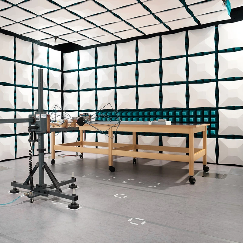
Reliability Through In-House EMC Testing
Our in-house EMC lab ensures that your electronic assemblies meet the highest standards.
Through thorough EMC testing, we identify sources of interference and develop corrective actions to ensure compliance with international regulations, shorten development times, and reduce costs.
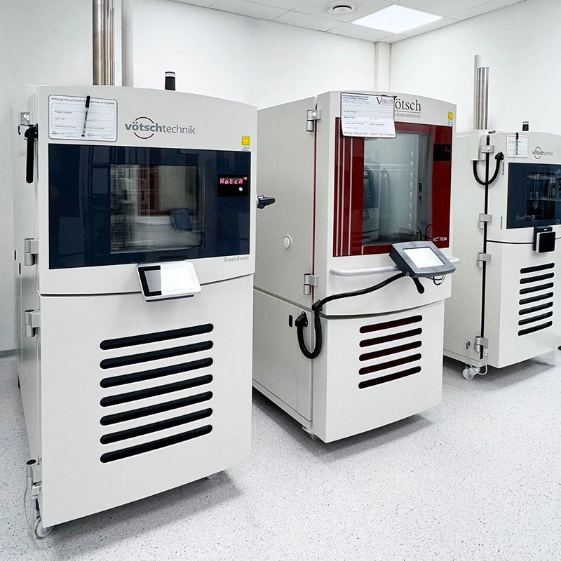
Precise Testing for Maximum Reliability
Our environmental laboratory tests your electronic components under extreme conditions using climate chambers, temperature shock chambers, and shakers.
We test according to common environmental standards, including temperature and humidity influences, to ensure the functionality and longevity of your products.
We are certified according to

ISO
14001:2015
IATF
16949:2016
ISO
9001:2015
TISAX®
We support you with expertise in design, software and hardware development, as well as the creation of efficient test strategies. Our goal is to perfect your products technically, align them with the highest quality standards, and place special emphasis on seamless production and cost efficiency.
Development Services
Enclosure Design and Simulations
Balancing form, function, and cost, we develop visually appealing enclosures to protect your electronics.Hardware
- Schematic Development
- PCB Layout
- Thermal Management Concepts & Simulations
Software
Embedded systems are our passion. With our expertise and modern software methods, we implement your product idea reliably and innovatively.Validation Laboratory
In-house laboratories for EMC measurements, environmental testing, vibration testing, and lifespan testing.Additional Services
- Material Procurement
- After-Sales Service
- Recycling/Disposal
- Obsolescence Management
- Repair